Quantum computing cluster emerging in Andhra; Fab, ATMP hubs emerging in Gujarat, Bhubaneswar: ISM CTO
Sep 09, 2026

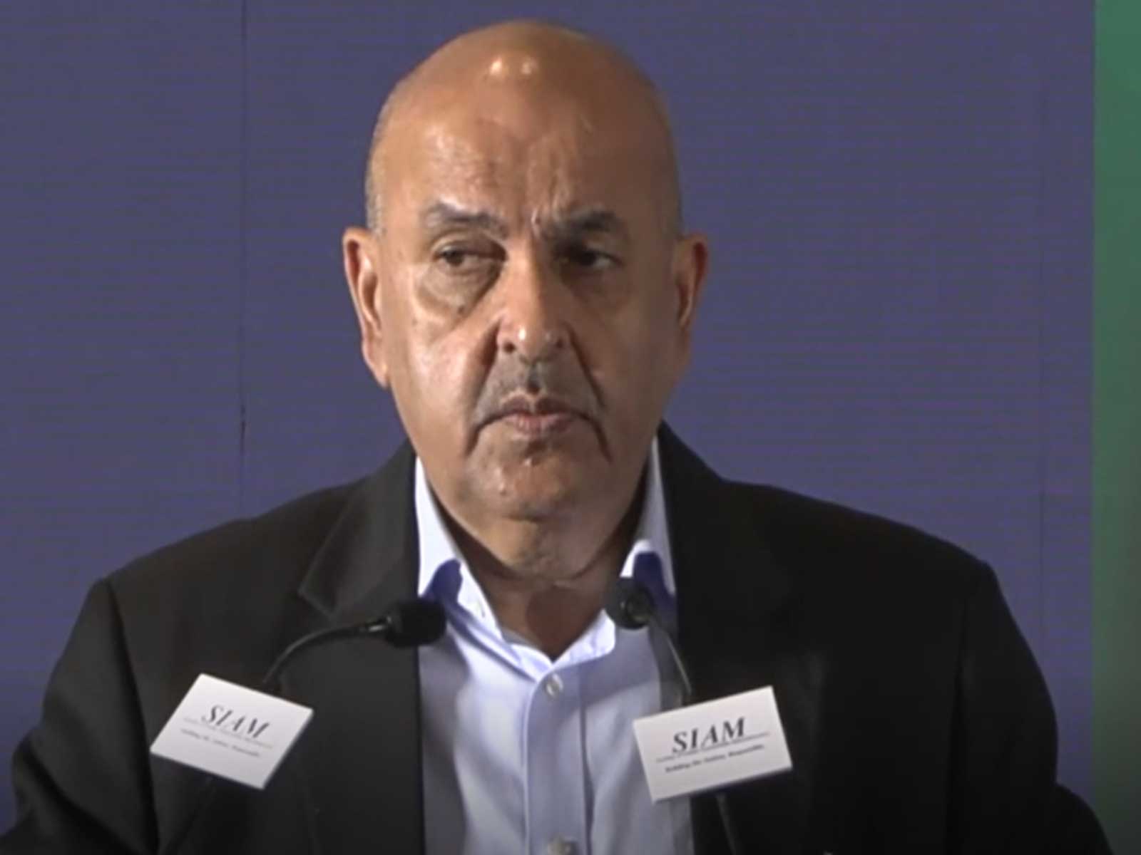
New Delhi [India], September 9 : India is witnessing the emergence of new semiconductor and advanced technology clusters, with quantum computing and photonics clusters emerging in Andhra Pradesh and fab and Assembly, Testing, Marking and Packaging (ATMP) clusters coming up in Gujarat and Bhubaneswar, India Semiconductor Mission (ISM) Chief Technology Officer Sarin Sundar said.
Addressing the launch of the India Photonics Association (IPA), an independent, ecosystem-led photonics industry body, on Wednesday, Sundar said the government expects the outlay under Semicon India 2.0 to be close to USD 40 billion. He, however, noted that the programme is still at an early stage and the estimates could change as more states come on board with additional support.
Highlighting the government’s push to develop technology clusters, Sundar cited Taiwan’s Hsinchu semiconductor ecosystem as a model for creating similar hubs across India.
“The clusters are being formed....the government's objective is very straightforward, if you see Taiwan that is Hsinchu, Hsinchu is where almost all the fabs are located in a small closed cluster, so we would like to have similar clusters at different places...so I think there is a very good quantum computing cluster coming out in Andhra Pradesh and also a photonics cluster somewhere in that area, so good fab clusters and ATMP (Assembly, Testing, Marking, and Packaging) clusters coming up in Gujarat and also in Bhubaneswar...” he said.
Sundar also highlighted developments around 3D glass, a substrate used in photonics, saying an Intel partner company, 3DGS, has secured “100% takeoff from Intel.”
“We also have 3D glass that is also a photonics substrate, that is having a 100% takeoff from Intel, that's an Intel partner company, 3DGS, and this is the current status of the approved projects,” he noted.
Referring to the capacity of semiconductor projects approved in the country, he said the Tata fab is expected to have a capacity of around 50,000 wafer starts per month, adding that details of the projects are available on the India Semiconductor Mission website.
India has launched its first independent, ecosystem-led photonics industry body, the India Photonics Association (IPA), to boost innovation, strengthen industry collaboration and fuel the country’s capabilities in the rapidly growing sector.
The industry body will serve as a neutral platform for collaboration and industry engagement and provide technically rigorous, industry-grounded inputs to support informed policymaking and strengthen India’s position in the global photonics ecosystem.